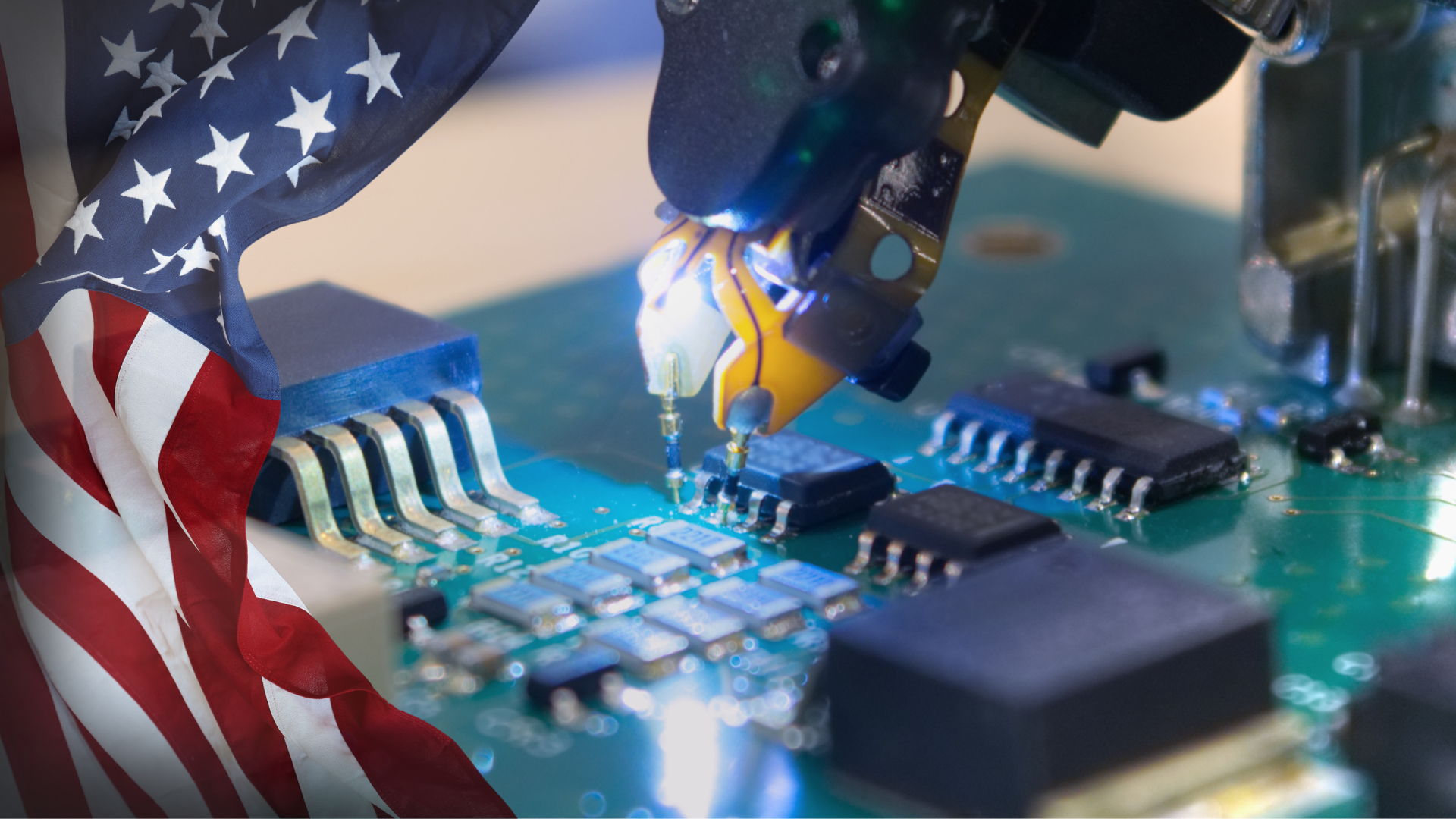
The semiconductor industry is undergoing a profound transformation, and at the center of this evolution is the rise of chiplets. While the concept is not entirely new, advances in design and manufacturing have made chiplets a practical and strategic approach to meeting today’s growing demand for performance, efficiency, and scalability.
As reported by EE Times:
“Conceptually it’s not new, but we are at a stage in chip design when complexity demands a more process-driven approach to designing with chiplets to reduce costs and development time, even though the use of multiple dies or chiplets creates new challenges.”
EE Times: Chiplets Consolidation Wave is Just Beginning
The Benefits of Chiplets
1. Flexibility
Chiplets allow manufacturers to source smaller, specialized dies from multiple vendors and combine them into a single package. This “build-your-own” model offers greater customization and design freedom than traditional monolithic chips.
2. Managing Complexity
As chips become more powerful, placing every function onto a single piece of silicon is increasingly difficult. By breaking designs into modular chiplets, development becomes more scalable, adaptable, and manageable.
3. Cost Efficiency
Producing one large, complex chip on a wafer can be costly and less efficient. Chiplets improve yield by enabling multiple smaller dies to be fabricated on the same wafer, lowering production costs and maximizing resource utilization.
The Challenges Ahead
Testing
Each chiplet must be rigorously tested and validated before integration. Ensuring compatibility and reliability across different chiplets is a critical step.
Reliability & Security
Because chiplets can come from multiple vendors, accountability becomes a concern. Who is responsible if a chiplet fails? Additionally, ensuring system-wide security across diverse sources is an ongoing challenge.
Looking to the Future
According to EE Times:
“A hybrid model will emerge where large players leverage proprietary solutions for their flagship products while engaging with open standards to tap into a broader ecosystem of innovation. The transition to optical I/O will mark the next great inflection point, promising to shatter current performance barriers.”
EE Times: Chiplets Consolidation Wave is Just Beginning
This signals a future where chiplets are not just an interim solution, but a fundamental building block of semiconductor innovation. As optical I/O and new standards emerge, chiplets will drive breakthroughs in performance, efficiency, and design flexibility.
Conclusion
Chiplets represent more than just a technological trend—they are shaping the next era of semiconductor design. With advantages in flexibility, scalability, and cost-effectiveness, alongside challenges in testing, reliability, and security, chiplets are poised to play a central role in the future of computing.
At Big Shine Korea, we continue to monitor these advancements closely to support our partners and clients with the latest insights and solutions in semiconductor distribution.